(in reverse chronological order)
 |
Piezoelectric microresonators for sensitive spin detection
Cecile Skoryna-Kline, Jorge Monroy Ruz and Krishna C. Balram
Physical Review Applied (2024)
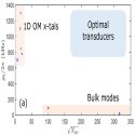
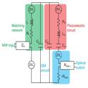
Piezoelectric microresonators are indispensable in wireless communications, and underpin radio-frequency filtering in mobile phones. These devices are usually analyzed in the quasi(electro)static regime with the magnetic field effectively ignored. On the other hand, at gigahertz frequencies and especially in piezoelectric devices exploiting strong dimensional confinement of acoustic fields, the surface magnetic fields can be significant. We demonstrate the existence of these surface magnetic fields in a proof-of-principle experiment and outline the prospects for sensitive spin detection using small-mode-volume piezoelectric microresonators, including the feasibility of electrical detection of single spins at cryogenic temperatures.
|
 |
Piezoelectric phononic integrated circuits
Krishna C. Balram
Applied Physics Letters (2024)
Piezoelectric microresonators have revolutionized modern wireless communication. While billions of these devices are in widespread use across a range of frequencies, materials, and device geometries, every piezoelectric microresonator in current use shares one common characteristic: they all manipulate (quasi) plane waves. Building on recent developments in related fields, in particular integrated photonics and quantum computing, we outline the prospects for piezoelectric phononic integrated circuits, which can manipulate gigahertz acoustic waves in micrometer-scale waveguide geometries in low-loss chipscale platforms.
|
 |
Robotic Vectorial Field Alignment for Spin-Based Quantum Sensors
Joe A Smith, Dandan Zhang and Krishna C. Balram
Advanced Science (2024)
Robotics has shown tremendous progress in realizing increasingly smart, autonomous, and highly dexterous machines. Here, a robotic arm equipped with a magnet is demonstrated to sensitize an NV center quantum magnetometer in challenging conditions unachievable with standard techniques.
|
 |
Low-Loss GHz Frequency Phononic Integrated Circuits in Gallium Nitride for Compact Radio Frequency Acoustic Wave Devices
Mahmut Bicer and Krishna C. Balram
IEEE Trans. Ultrasonics, Ferroelectrics and Freq. Control (2023)
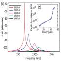
Guiding and manipulating GHz frequency acoustic waves in μm -scale waveguides and resonators open up new degrees of freedom to manipulate radio frequency (RF) signals in chip-scale platforms. A critical requirement for enabling high-performance devices is the demonstration of low acoustic dissipation in these highly confined geometries. We demonstrate ultra-low loss acoustic microring resonators and compact spiral delay lines with microwave signal delays exceeding 750 m.
|
 |
Heterogeneous Integration of Solid-State Quantum Systems with a Foundry Photonics Platform
Hao-Cheng Weng, Jorge Monroy-Ruz, Jonathan C.F. Matthews, John G. Rarity, Krishna C. Balram and Joe A. Smith
ACS Photonics (2023)
we demonstrate the heterogeneous integration of NV centers in nanodiamond with low-fluorescence silicon nitride photonics from a standard 180 nm CMOS foundry process. Nanodiamonds are positioned over predefined sites in a regular array on a waveguide in a single postprocessing step. Using an array of optical fibers, we excite NV centers selectively from an array of six integrated nanodiamond sites, collect the photoluminescence (PL) in each case into waveguide circuitry on-chip and verify single photon emission by an on-chip Hanbury Brown and Twiss cross-correlation measurement.
|
 |
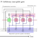
Timing Constraints Due to Real-Time Graph-Traversal Algorithms on Incomplete Cluster States in Photonic Measurement-Based Quantum Computing
John Scott and Krishna C. Balram
Physical Review Applied (2023)
Understanding the computational overheads imposed by classical control systems on quantum computing platforms becomes critically important as these quantum machines grow in scale and complexity. In this work, we calculate the overheads imposed by the implementation of real-time graph traversal algorithms needed to find computational paths through incomplete cluster states for the implementation of one-qubit gates; a necessary requirement for a realistic implementation of photonic measurement-based quantum computing. We also analyze the trade-off between the accuracy of finding viable paths and the speed at which this operation can be performed, which constrains the overall photonic clock cycle of the system.
|
 |
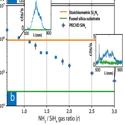
Quantifying and mitigating optical surface loss in suspended GaAs photonic integrated circuits
Robert Thomas, Haoyang Li, Pisu Jiang and Krishna C. Balram
Optics Letters (2023)
Understanding and mitigating optical loss is critical to the development of high-performance photonic integrated circuits (PICs). In particular, in high refractive index contrast compound semiconductor (III–V) PICs, surface absorption and scattering can be a significant loss mechanism, and needs to be suppressed. Here, we quantify the optical propagation loss due to surface state absorption in a suspended GaAs PIC platform, probe its origins using x-ray photoemission spectroscopy and spectroscopic ellipsometry, and show that it can be mitigated by surface passivation using alumina.
|
 |
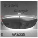
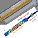
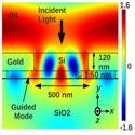
Piezo-Optomechanical Signal Transduction Using Lamb-Wave Supermodes in a Suspended GalliumArsenide Photonic-Integrated-Circuit Platform
Ankur Khurana, Pisu Jiang and Krishna C. Balram
Physical Review Applied (2022)
Piezoelectric optomechanical platforms present one of the most promising routes towards efficient transduction of signals from the microwave to the optical frequency domains. While there has been significant recent progress particularly on the materials front, alternative device architectures that can potentially meet the stringent efficiency requirements of quantum transducers need to be continuously explored. Here, we utilize the mechanical supermode principle to improve the overall microwave-to-optical transduction efficiency, by fabricating Lamb-wave resonators that are hybridized with the mechanical breathing modes of a rib waveguide in a suspended gallium arsenide photonic-integrated-circuit platform.
|
 |
Using electrical resistance asymmetries to infer the geometric shapes of foundry patterned nanophotonic structures
Vinita Mittal and Krishna C. Balram
Optics Express (2022)
While silicon photonics has leveraged the nanofabrication tools and techniques from the microelectronics industry, it has also inherited the metrological methods from the same. Photonics fabrication is inherently different from microelectronics in its intrinsic sensitivity to 3D shape and geometry, especially in a high-index contrast platform like silicon-on-insulator. In this work, we show that electrical resistance measurements can in principle be used to infer the geometry of such nanophotonic structures and reconstruct the micro-loading curves of foundry etch processes.
|
 |
Toward compact high-efficiency grating couplers for visible wavelength photonics
Joe Smith, Jorge Monroy-Ruz, Pisu Jiang, John G. Rarity, and Krishna C. Balram
Optics Letters (2022)
Although grating couplers have become the de-facto standard for optical access to integrated silicon photonics platforms, their performance at visible wavelengths, in moderate index contrast platforms such as silicon nitride, leaves significant room for improvement. In particular, the index contrast governs the diffraction efficiency per grating tooth and the resulting overall coupler length. In this work, we develop two approaches to address this problem: a dielectric grating that sums multiple optical modes to increase the overall output intensity; and an embedded metal grating that enhances the attainable refractive index contrast, and therefore reduces the on-chip footprint.
|
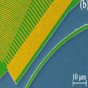 |
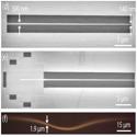
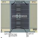
Gallium nitride phononic integrated circuits platform for GHz frequency acoustic wave devices
Mahmut Bicer, Stefano Valle, Jacob Brown, Martin Kuball, and Krishna C. Balram
Applied Physics Letters (2022)
Strong transverse confinement of high-frequency sound and low-loss routing in on-chip waveguides will bring new degrees of freedom to manipulate GHz frequency acoustic waves, analogous to the change brought forth by silicon integrated photonics to the routing and manipulation of light on a chip. We demonstrate that high frequency (>3GHz) sound can be efficiently guided in μm-scale gallium nitride (GaN) waveguides and ring resonators by exploiting the strong velocity contrast available in the GaN on silicon carbide (SiC) platform.
|
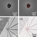 |
Smooth Sidewalls on Crystalline Gold through Facet-Selective Anisotropic Reactive Ion Etching: Toward Low-Loss Plasmonic Devices
Alexander Greenwood, Krishna C. Balram and Henkjan Gersen
Nano Letters (2022)
Quantum plasmonics aims to harness the deeply subwavelength confinement provided by plasmonic devices to engineer more efficient interfaces to quantum systems in particular single emitters. Realizing this vision is hampered by the roughness-induced scattering and loss inherent in most nanofabricated devices. We show evidence of a reactive ion etching process to selectively etch gold along select crystalline facets.
|
 |
Timing Constraints Imposed by Classical Digital Control Systems on Photonic Implementations of Measurement-Based Quantum Computing
John R. Scott and Krishna C. Balram
IEEE Transactions in Quantum Engineering (2022)
Most of the architectural research on photonic implementations of measurement-based quantum computing (MBQC) has focused on the quantum resources involved in the problem with the implicit assumption that these will provide the main constraints on system scaling. However, the “flying-qubit” architecture of photonic MBQC requires specific timing constraints that need to be met by the classical control system and their implications for photonic quantum computing.
|
 |
Piezoelectric Optomechanical Approaches for Efficient Quantum Microwave-to-Optical Signal Transduction: The Need for Co-Design
Krishna C. Balram, and Kartik Srinivasan
Wiley Advanced Quantum Technologies (2022)
Piezoelectric optomechanical platforms represent one of the most promising routes toward achieving quantum transduction of photons between the microwave and optical frequency domains. However, there are significant challenges to achieving near-unity transduction efficiency. We discuss such factors in the context of the two main approaches being pursued for high efficiency transduction.
|
 |
Nitrogen-vacancy center coupled to an ultrasmall-mode-volume cavity: A high-efficiency source of indistinguishable photons at 200 K
Joe Smith, Chloe Clear, Krishna C. Balram, Dara McCutcheon and John Rarity
Physical Review Applied (2021)
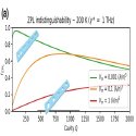
Solid-state atomlike systems have great promise for linear optic quantum computing and quantum communication but are burdened by phonon sidebands and broadening due to surface charges. Nevertheless, coupling to a small-mode-volume cavity would allow high rates of extraction from even highly dephased emitters. We consider the nitrogen-vacancy center in diamond, a system understood to have a poor quantum optics interface with highly distinguishable photons, and design a silicon nitride cavity that allows 99% efficient extraction of photons at 200 K with an indistinguishability of >50%, improvable by external filtering.
|
 |
Suspended gallium arsenide platform for building large scale photonic integrated circuits: passive devices
Pisu Jiang and Krishna C. Balram
Optics Express (2020)
The spectacular success of silicon-based photonic integrated circuits (PICs) in the past decade naturally begs the question of whether similar fabrication procedures can be applied to other material platforms with more desirable optical properties. In this work, we demonstrate the individual passive components (grating couplers, waveguides, multi-mode interferometers and ring resonators) necessary for building large scale integrated circuits in suspended gallium arsenide (GaAs).
|
 |
Single photon emission and single spin coherence of a nitrogen vacancy center encapsulated in silicon nitride
Joe Smith, Jorge Monroy-Ruz, John Rarity and Krishna C. Balram
Applied Physics Letters (2020) Editor's Pick
Finding the right material platform for engineering efficient photonic interfaces to solid state emitters has been a long-standing bottleneck for scaling up solid state quantum systems. In this work, we demonstrate that nitrogen rich silicon nitride, with its low auto-fluorescence at visible wavelengths, is a viable quantum photonics platform by showing that nitrogen vacancy centers embedded in nanodiamonds preserve both their quantum optical and spin properties post-encapsulation.
|
 |
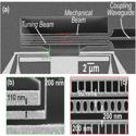
Microwave-to-Optical Transduction Using a Mechanical Supermode for Coupling Piezoelectric and Optomechanical Resonators
Marcelo Wu, Emil Zeuthen, Krishna C. Balram and Kartik Srinivasan
Physical Review Applied (2020)
Spurred by recent developments in quantum information, there has been a lot of interest in the development of quantum transducers for efficient, low-noise, and bidirectional frequency conversion of photons between the microwave and optical domains. We propose to realize such functionality through the coupling of electrical, piezoelectric, and optomechanical resonators. The coupling of the mechanical subsystems enables formation of a resonant mechanical supermode that provides a mechanically mediated, efficient single interface to both the microwave and optical domains.
|
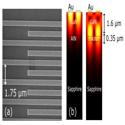 |
High frequency guided mode resonances in mass-loaded, thin film gallium nitride surface acoustic wave devices
Stefano Valle, Manikant Singh, Martin Cryan, Martin Kuball and Krishna C. Balram
Applied Physics Letters (2019) Editor's Pick
We demonstrate high-frequency (>3 GHz), high quality factor radio frequency (RF) resonators in unreleased thin film gallium nitride (GaN) on sapphire and silicon carbide substrates by exploiting acoustic guided mode (Lamb wave) resonances. The GaN platform, with its ability to guide and localize high-frequency sound on the surface of a chip with access to high-performance active devices, will serve as a key building block for monolithically integrated RF front-ends.
|
 |
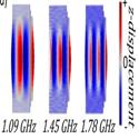
Elimination of thermomechanical noise in piezoelectric optomechanical crystals
Hugh Ramp, Bradley Hauer, Krishna C. Balram, et al.
Physical Review Letters (2019)
We eliminate thermomechanical noise in the GHz-frequency mechanical breathing mode of a piezoelectric optomechanical crystal using cryogenic cooling in a dilution refrigerator. We optically measure an average thermal occupancy of the mechanical mode of only
0.7 ± 0.4 phonons, providing a path towards low-noise microwave-to-optical conversion in the quantum regime.
|
 |
High-frequency, resonant acousto-optic modulators fabricated in a MEMS foundry platform
Stefano Valle and Krishna C. Balram
Optics Letters (2019)
We report the design and characterization of high-frequency, resonant acousto-optic modulators (AOMs) in a micro-electro-mechanical systems (MEMS) foundry process. The doubly resonant cavity design, with short acoustic and optical cavity lengths, allows us to measure acousto-optic modulation at GHz frequencies with high modulation efficiency. In contrast to traditional AOMs, these devices rely on the perturbation induced by the displacement of cavity boundaries, which can be significantly enhanced in a suspended geometry.
|
 |
The 2019 surface acoustic waves roadmap: Cavity optomechanics with surface acoustic waves
Kartik Srinivasan, Marcelo Wu and Krishna C. Balram
Journal of Physics D: Applied Physics (2019)
We summarize the opportunities and potential roadblocks presented by the adoption of piezoelectric material platforms for cavity optomechanics.
|
 |
Tuning and stabilization of optomechanical crystal cavities through NEMS integration
Karen E. Grutter, Marcelo I. Davanco, Krishna C. Balram, and Kartik Srinivasan
APL Photonics (2018) Invited article
We demonstrate the electrostatic tuning and stabilization of optomechanical devices, by integrating a Si3N4 slot-mode optomechanical crystal cavity with a nanoelectromechanical systems element, which controls the displacement of an additional “tuning” beam within the optical near-field of the optomechanical cavity.
|
 |
Acousto-Optic Modulation and Optoacoustic Gating in Piezo-Optomechanical Circuits
Krishna C. Balram, Marcelo I. Davanço, B. Robert Ilic, Ji-Hoon Kyhm, Jin Dong Song, and Kartik Srinivasan
Physical Review Applied (2017)
We extend our prior work on piezo-optomechanical circuits by studying dynamical effects in these circuits. We demonstrate acousto-optic modulation and optoacoustic gating (the inverse effect), in which the application of modulated optical pulses interferometrically gates the transmission of propagating acoustic pulses.
|
 |
Efficient fiber-coupled single-photon source based on quantum dots in a photonic-crystal waveguide
Raphaël S. Daveau, Krishna C. Balram, et al.
Optica (2017)
We demonstrate an efficient fiber-coupled photonic-crystal waveguide (PCWG) based single-photon source by optimizing the evanescent coupling of the light field between the tapered waveguide and a tapered optical fiber. The coupling is robust, stable, and broadband.
|
 |
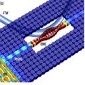
Coherent coupling between radiofrequency, optical and acoustic waves in piezo-optomechanical circuits
Krishna C. Balram, Marcelo I. Davanço, Jin Dong Song, and Kartik Srinivasan
Nature Photonics (2016)
We develop a platform for nanoscale cavity optomechanical circuits in which optomechanical cavities supporting co-localized 1,550 nm photons and 2.4 GHz phonons are combined with photonic and phononic waveguides.
|
 |
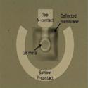
Moving boundary and photoelastic coupling in GaAs optomechanical resonators
Krishna C. Balram, Marcelo I. Davanço, Ju Young Lim, Jin Dong Song, and Kartik Srinivasan
Optica (2014)
We develop GaAs optomechanical resonators and investigate the relative contributions of moving dielectric boundaries and the photoelastic effect to the optomechanical coupling rate.
|
 |
Surface-Normal Ge-SiGe Asymmetric Fabry–Perot Optical Modulators Fabricated on Silicon Substrates
Ross M. Audet, Elizabeth H. Edwards, Krishna C. Balram et al.
IEEE Journal of Lightwave Technology (2013)
We demonstrate the first vertical-incidence Ge-SiGe quantum well reflection modulators fabricated entirely on standard silicon substrates. These modulators could help enable massively parallel, free-space optical interconnects to silicon chips.
|
 |
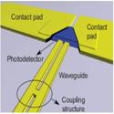
Nanoscale resonant-cavity-enhanced germanium photodetectors with lithographically defined spectral response for improved performance at telecommunications wavelengths
Krishna C. Balram, Ross M. Audet, and David A. B. Miller
Optics Express (2013)
We demonstrate the use of a subwavelength planar metal-dielectric resonant cavity to enhance the absorption of germanium photodetectors at wavelengths beyond the material’s direct absorption edge, enabling high responsivity across the entire telecommunications C and L bands.
|
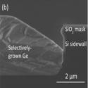 |
Selective area growth of germanium and germanium-silicon-germanium quantum wells in silicon waveguides for on-chip optical interconnect applications
S. A. Claussen, Krishna. C. Balram, E. T. Fei, T. I. Kamins, J. S. Harris, and D. A. B. Miller
Optical Materials Express (2012)
We propose a robust fabrication process for growing Ge and Ge-based heterostructures in growth windows with Si sidewalls which can be applied to growth in thick Si optical waveguides.
|
 |
Self-aligned silicon fins in metallic slits as a platform for planar wavelength-selective nanoscale resonant photodetectors
Krishna C. Balram, and David A. B. Miller
Optics Express (2012)
We propose and demonstrate a novel nanoscale resonant metal-semiconductor-metal (MSM) photodetector structure based on silicon fins self-aligned to metallic slits. This geometry allows the center wavelength of the photodetector’s spectral response to be controlled by the silicon fin width, allowing multiple detectors, each sensitive to a different wavelength, to be fabricated in a single-step process.
|
 |
Routing and photodetection in subwavelength plasmonic slot waveguides
Dany-Sebastien Ly-Gagnon, Krishna C. Balram, et al.
Nanophotonics (2012)
We demonstrate a photodetector linked to a two conductor metallic slot waveguide that supports a mode with a minute cross-sectional area of λ^2/100 and propagation lengths of 10λ (λ = 850 nm).
|
 |
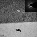
Strained germanium thin film membrane on silicon substrate for optoelectronics
Donguk Nam, Devanand Sukhdeo, Arunanshu Roy, Krishna C. Balram, et al.
Optics Express (2011)
We present a novel method to introduce a sustainable biaxial tensile strain larger than 1% in a thin Ge membrane using a stressor layer integrated on a Si substrate.
|
 |
Tensile-strained germanium-on-insulator substrate fabrication for silicon-compatible optoelectronics
J. Raja Jain, Dany-Sebastien Ly-Gagnon, Krishna C. Balram, et al.
Optical Materials Express (2011)
We present a method to fabricate tensile-strained germanium-on-insulator (GOI) substrates using heteroepitaxy and layer transfer techniques
|
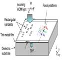 |
Multiple-Wavelength Focusing of Surface Plasmons with a Nonperiodic Nanoslit Coupler
Takuo Tanemura, Krishna C. Balram, et al.
Nano Letters (2011)
An array of nanoslits patterned on a thin metal film is used to couple free-space light into surface plasmon polaritons (SPPs) and simultaneously focus different-wavelength SPPs into arbitrary predefined locations in the two-dimensional plane.
|
|